Programmable Dual LDO Output Voltage and WLED Current with I2C Interface
1. Introduction
The RT9367A is an integrated solution for panel backlighting and phone camera application. The part contains a charge pump white LED driver and dual low dropout linear regulators. The RT9367A application mechanism and I2C compatible interface are introduced in this application note.
2. Dual LDO Camera Supply Input
In the section of linear regulator, the RT9367A comprises a dual channel, low noise, and low dropout regulator sourcing up to 300mA at each channel for phone camera input voltage supply. The output voltage range of each channel can be configured from 1.1V to 3.3V by I2C interface. The latest cell-phone usually integrates two sets of embedded cameras. One is major camera and the other one is the secondary camera. For camera phone users, those two camera sets will not be used at the same time. Beside, each camera needs two different input voltages. In order to achieve the above-mentioned goal, four different voltage linear regulators are needed in traditional power management topology, and this will increase space and cost. However, the RT9367A can realize this application by its integrated programmable Dual LDO. Figure 1 shows the application circuit of dual LDO. The inputs of Camera A and Camera B are connected in parallel to LDO1 and LDO2. The input voltage level of Camera A and B could be different. Users can change the LDO1 and LDO2 output voltage for Camera A or Camera B via I2C interface. Notice that, both of Camera A and Camera B must be able to withstand the maximum input voltage (3.3V). Due to the above-mentioned reason, the RT9367A provides a highly integrated solution that greatly reduces components and PCB space.
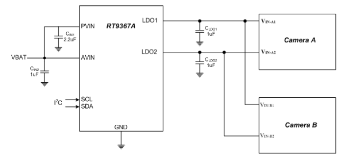
Figure 1. Dual LDO Camera Supply Input Applicaiton Circuit
3. Charge Pump LED Driver
The part contains highly integrated, 1MHz, low noise, high efficiency 1x/1.5x/2x multimode charge pumps and low dropout current regulators for driving W-LED backlighting. The RT9367A can power up 4 white LEDs with regulated constant current for uniform intensity as shown in the figure 2. Each channel (LED1-LED4) can support current up to 25mA. An internal 5-bit DAC is used for brightness control, so that users can easily configure up to 32-step of LED current by the I2C interface. The RT9367A charge pumps feature low-noise constant-frequency operation and automatically optimize efficiency based on VIN and LED forward voltage conditions. The devices power up in 1x mode and automatically switch to boost mode (1.5x) when any enabled LED current source approaches dropout; a subsequent dropout switches the parts into 2x mode. The internal circuitry prevents inrush current and excessive input noise during start-up and mode switching. In addition, the device has short circuit, thermal and open/short LED protection.
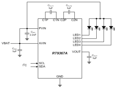
Figure 2. Charge Pump LED Driver Application Circuit
4. I2C Compatible Interface
4-1 I2C Interface Timing Diagram
The RT9367A acts like an I2C -bus slave. The I2C -bus master configures the settings for Dual LDO and the LED outputs by sending command bytes to the RT9367A via the 2-wire I2C -bus. Figure 3 shows the timing diagram of I2C interface. After the START condition, the I2C master sends a chip address. This address is seven bits long followed by an eighth bit which is a data direction bit (R/W). The second byte selects the register to which the data will be written. The third byte contains data to write to the selected register.
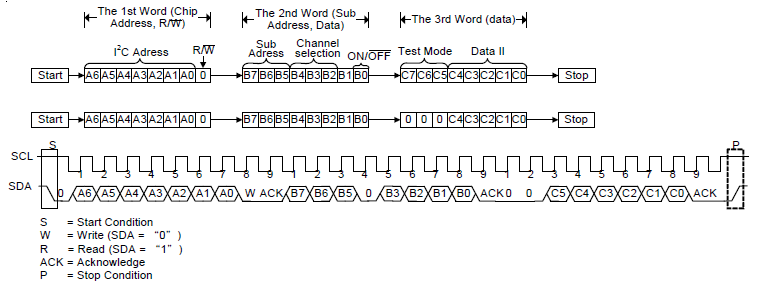
Figure 3. I2C Interface Timing Diagram
4-2 LDO Output Voltage and LED Current Setting
In the first byte, the RT9367A address is 1010100 (54h) and a receive-only device. Figure 4 shows the writing information for RT9367A dual LDO output voltage setting and LED current setting. In the second byte, the sub-address of dual LDO is "001" and the sub-address of LED Driver is "010". For LDO channel setting, the LDO1 is defined as "000" and the LDO2 is defined as "001". For the last bit of second byte, a "0" indicates a DISABLE and a "1" indicates an ENABLE function. The sub-address of LED is "010". For the last 4 bits (B0 to B3) represent the channels of LED (LED1 to LED4), a "0" indicates turn off and a "1" indicates turn on. The data of third byte (C0 to C4) indicates a 32-steps setting of LDO1, LDO2 output voltage or the LED current of backlight.
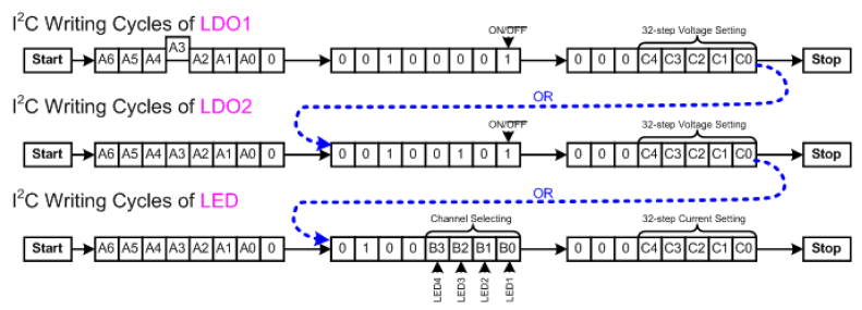
Figure 4. I2C Writing Cycles for LDO and LED Driver
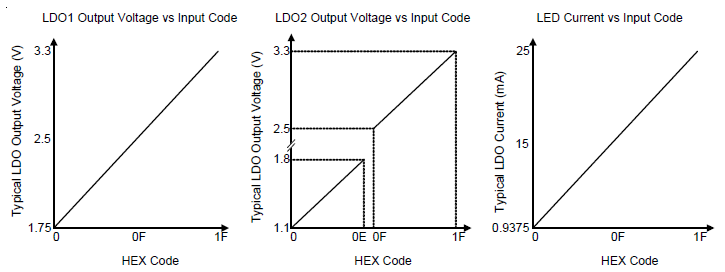
Figure 5. LDO Voltage Setting and LED Current Setting
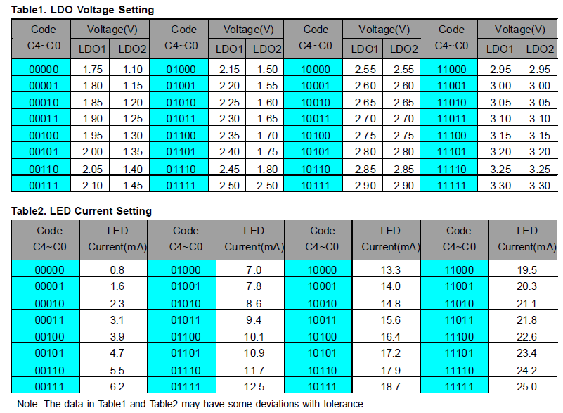
Figure5, Table1 and Table2 illustrate the dual LDO output voltage and LED current setting information. The output voltage of the LDO1 could be divided to 32-step levels between 1.75V(HEX Code = 0) and 3.3V(HEX Code = 1F). And the output voltage of the LDO2 is separated into two regions, one is from 1.1V(HEX Code = 0) to 1.8V(HEX Code = 0E) and the other is from 2.5V(HEX Code = 0F) to 3.3V(HEX Code = 1F). In additional, the LED current could be divided into 32-step levels between 0.8mA(HEX Code = 0) and 25mA(HEX Code = 1F).
4-3 Design Examples
An example shows as below to demonstrate the setting of RT9367A LED current and the Dual LDO output voltage. For the following examples the RT9367A address is 1010100 (54h) which is the first byte. As shown in above-mentioned, the sub-address of Dual LDO is 001 and LED is 010.
Example:
LDO1 output voltage = 2.8V
LDO2 output Voltage = 1.2V
LED1 to LED3 ON current = 25mA
LED4 OFF
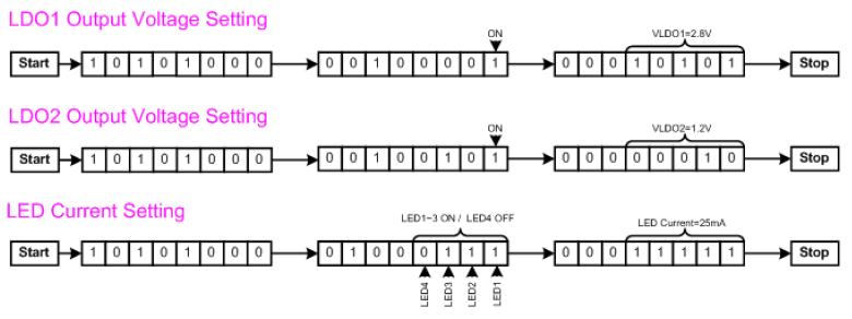
Figure 6. LDO Voltage and LED Current Programming via I2C
5. Layout Consideration
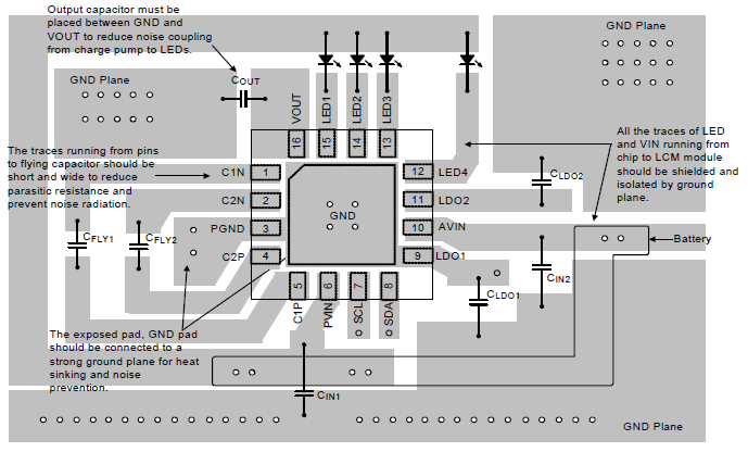
The RT9367A is a high-frequency switched-capacitor converter and a careful PCB layout is necessary for optimal performance. At first, place all peripheral components as close to the IC as possible. And then place CIN1, CIN2, COUT, CLDO1, CLDO2, CFLY1, and CFLY2 near to AVIN, PVIN, VOUT, LDO1, LDO2, C1P, C1N, C2P, C2N, and GND pin respectively. Besides, a shorter connection is highly recommended. The following guidelines should be strictly followed when designing a PCB layout for the RT9367A.
- The exposed GND pad must be soldered to a large
ground plane for heat sinking and noise prevention.
- VIN traces should be wide enough to minimize
inductance and handle the high currents.
- The input and output capacitors must be placed close
to the part.
- The flying capacitors must be placed close to the
part. The traces running from the pins to the capacitor pads should be as
wide as possible. Long traces will also produce large noise radiation
caused by the large dv/dt on these pins. So the short trace is
recommended.
- All the traces of LED and VIN running from pins to
LCM module should be shielded and isolated by ground plane. The shielding
prevents the interference of high frequency noise coupled from the charge
pump.
- The output capacitor must be placed between GND and
VOUT to reduce noise coupling from charge pump to LEDs.
6. Conclusion
The I2C interface is widely adopted on smart hand-held devices due to its convenience and stability. The RT9367A adopts I2C programming mechanism to provide an excellent solution with advantages in terms of component reducing, PCB space saving, and convenient control.